Join Us Institute Profile

Institute Profile

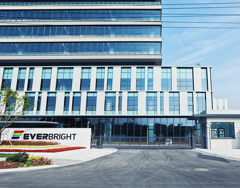
EVERBRIGHT INSTITUTE OF SEMICONDUCTOR PHOTONICS CO., LTD.

Everbright Institute Of Semiconductor Photonics Co., Ltd. (“the Institute”), founded in March 2018, was jointly established by Suzhou Everbright Photonics Co., Ltd. (“Everbright Photonics”) and the Government of Suzhou National New & Hi-tech Industrial Development Zone. As a research and innovation platform built by Everbright Photonics, the Institute fully utilizes Everbright Photonics’ cutting-edge chip R&D and manufacturing technology platform. It is committed to cultivating and introducing a group of high-level talents and industrialization projects related to semiconductor lasers and optoelectronics, building a professional platform for incubating and industrializing achievements in the field of semiconductor optoelectronic devices such as semiconductor lasers, and becoming a science and technology innovation highland and industrial base with international influence in semiconductor laser chips and related fields.

The Institute adopts an innovative model of “government guidance and support + enterprise management and operation” to reasonably and fully leverage the role and efficiency of government departments and market entities in industrial innovation. The Institute is not only the strategic implementation subject of Everbright Photonics’ “one platform, one fulcrum, horizontal expansion, and vertical extension”, but also the core construction partner of Suzhou High-tech Zone in building an innovative cluster for the semiconductor laser industry.

The first phase of the Institute covers an area of about 35 mu (one mu = 0.0667 hectares), including R&D Building, Production Process Building, Comprehensive Building, Power Building, and Class A Warehouse, etc., with a building area of about 50,000 square meters and a total investment of RMB 500 million, including RMB 300 million for civil works. The Institute launched the construction of Phase II advanced compound semiconductor optoelectronic platform in 2023. That project covers an area of about 30 mu, with a building area of about 46,000 square meters and a total investment of RMB 1 billion. It is expected to be put into operation in 2025.

The Institute has enough instruments and equipment to provide testing and process development services for compound semiconductors and related fields, including (but not limited to) material and device testing and analysis, epitaxial process services, chip process services, optoelectronic device packaging, and so on. Everbright Photonics has built and operated the first domestically and the second globally advanced six-inch GaAs optoelectronic device production line, with strong testing and process service capabilities. It will continue to inject great forces to the development of Suzhou’s photon industry in the future.


The “Key Technologies and Industrialization of High Brightness, Long Life, and High Power Semiconductor Laser Chips” project of the Institute won the first prize of Jiangsu Provincial Science and Technology Award in 2021. The Institute was recognized as a “National High-tech Enterprise”, “Innovative SME”, and “Jiangsu Private Science and Technology Enterprise” in 2023. In terms of patents, the Institute has 111 patents in force, including 86 invention patents, 21 utility model patents, and 3 design patents, and 1 PCT patent. “A high-power semiconductor chip and its preparation method”, an invention patent of the Institute, won the 24th China Patent Excellence Award.

Organizational Structure

Industry-University-Research Cooperation

To strengthen the cutting-edge physical basis and technical research of GaN lasers, and comprehensively improve the R&D level of GaN lasers, the Institute launched the industry-university-research cooperation with Suzhou Institute of Nano-Tech and Nano-Bionics, Chinese Academy of Sciences, to jointly build the “GaN Laser Joint Laboratory”.

Join Us

Recruitment

All positions(Tools 17)

MOCVD Engineer

Full-time | Suzhou | Unlimited

2024-03-05

Job responsibilities:

1. Develop MOCVD processes for GaAs- and InP-based lasers and other semiconductor devices.
2. Document operational procedures and protocols, and assist with continual improvement. Focusing on improving yield, reproducibility and utilization rate.
3. Inspect and characterize semiconductor wafers using multiple metrology techniques including XRD,PL,ECV,Hall,TEM,and SIMS etc..
4. Train personnel for the development and manufacturing on MOCVD tools.
5. Support and interact with other departments and manufacturing personnel for production.
6. Manage Advanced Technology Program, including experiment design, data analysis, progress management, result summary and report。Writing relevant papers and patents for the publication.

Job qualifications:

1. PHD in Science or Engineering Discipline (Materials Science, Physics, Chemical Engineering or Electrical Engineering).
2. 1-3 years hands-on MOCVD experiences, particularly in the development and manufacturing of GaAs- and InP-based lasers.
3. Familiar with device physics and the design of GaAs- and InP-based lasers.
4. Knowledge and expertise in material characterization and metrology equipment, including XRD,PL,ECV,Hall,TEM,SIMS, etc..
5. Must be proficient in MS office, familiar with DOE analysis, and have excellent engineering documentation skills and communication skills.
6. Experience with the development of VCSEL and Tunnel Junction devices is preferred.

If you are interested, you may send your resume to :hr@everbrightphotonics.com
MBE

Full-time | Suzhou | Unlimited

2024-03-05

Job responsibilities:

1. Responsible for UHV-MBE epitaxial growth of III-V semiconductor devices. Develop the products with competitive performance and cost, by optimizing the MBE process and device structure.
2. Establish a production quality control system for R&D products. Find and solve the problems during the R&D and production. Improve the yield and equipment utilization.
3. Analysis of epitaxial materials, by RHEED, TEM, XRD, AFM, PL, SIMS, ECV, SEM, etc.
4. Train and guide operators and engineers to carry out extended production and research and development.
5. Support the safe production operation of the department.
6. Responsible for the application and management of the company's R&D projects, including designing experiments, analyzing data, project progress control, summarizing and reporting results, publishing papers and apply for patents, project concluding reports as required.

Job qualifications:

1. Doctoral degree (Materials, physics, Electronics), or master degree, proficient experience is preferred.
2. With an in-depth understanding and rich experience in the MBE growth and structural characterization of compound semiconductors is preferred. Proficiency with MBE equipment and techniques, including UHV system, able to find and solve problems, upgrade, and transform equipment.
3. Familiar with III-V semiconductor device design. Experience in semiconductor device R&D based on GaAs and InP is preferred, experience in semiconductor laser device R&D and epitaxial design is preferred.
4. Proficient or familiar with one or more material analysis techniques in RHEED, TEM, XRD, AFM, PL, SIMS, ECV, SEM etc.
5. Proficiency with data statistics and analysis software, familiar with DOE analysis.
6. Strong desire to work in a collaborative team environment. High engineering communication skills, ability to work flexible hours.

If you are interested, you may send your resume to :hr@everbrightphotonics.com
Device Engineer

Full-time | Suzhou | Unlimited

2024-03-05

Job responsibilities:

1.Researching and Developing lasers diode devices and related technologies with world-class performance, and cost competitivity.
2.Participating in device performance improvement and new product certification, including Design epitaxy and device structure and reliability certification.
3.Master the fabrication process of GaAs and InP lasers diode, with 1-2 specialties. Master the device testing, failure analysis.
4.Participating in or manage project application and Implementation. Analyzing, summarizing and reporting the progress of experiments and projects, writing articles and patents

Job qualifications:

1.Doctoral degree in semiconductor optoelectronics;
2.Semiconductor device design, test and analysis ability;
3.3-5 years of semiconductor laser devices and product R & D experience;

If you are interested, you may send your resume to :hr@everbrightphotonics.com
Optical engineer

Full-time | Suzhou | Unlimited

2024-03-05

Job responsibilities:

1.Develop advanced diode laser beam shaping, beam combining, wavelength stabilizating and measuring technologies ;
2. Develop cutting-edge and cost competitive fiber-coupled and free-space products;
3. Patent developed technologies and products. Publish such developments in conferences and journals.
4.Lead NPI(New Product Instruction)of optical products before beta stage;
5. Provide technical support for volume production;
6. Lead project application and execution.Work proactively with other cooperation companies and institutes.
7.Teach and train product engineers and process engineesr.

Job qualifications:

1.PhD degree in optics / photonics, physics, Engineering or related majors;
2. Familiar with at least one programming language: MATLAB, C + +, C # / VB,. Net and LabVIEW;
3. Open-mined,self-motivated and quick-learning.

If you are interested, you may send your resume to :hr@everbrightphotonics.com
Fabrication process engineer

Full-time | Suzhou | Unlimited

2024-03-05

Job responsibilities:

1. Develops new processes.
2. Participates the installation, the debugging, and creating the standard operating procedure (SOP) for 6 inches equipment.
3. Participates the development and optimization of fabrication processes for new products.
4. Supports the design, analysis and report for the process experiments.
5. Supports equipment maintenance and troubleshooting of existing production line.
6. Creates documentation, paper, and patent for projects. 7. Accomplishes works from directors.

Job qualifications:

1. Master or PHD in Materials Science, Chemical Engineering Physics or related field (Mechanical Engineering,Optics, etc.).
2.Prior experience on wafer fabrication process and equipment.
3.Strong problem/trouble shooting skills.
4.Ability to work in either a team or independent environment.
5. Effective communication skills.

If you are interested, you may send your resume to :hr@everbrightphotonics.com
Sales Engineer

Full-time | Suzhou | Unlimited

2024-03-05

Job responsibilities:

1. Conduct market development, sales, and customer maintenance to promote the company’s products being distributed to domestic and foreign universities, research institutes, semiconductor manufacturers, and so on;
2. Collect market and industry information, set up sales targets based on market demand, and decompose sales tasks;
3. Develop sales channels, actively participate in industry exchanges, promote company products and services, develop new customers, explore market demand, and formulate new plans;
4. Communicate solutions and engage in business negotiations with clients, coordinate bidding projects, prepare bidding documents, and sign contracts;
5. Follow up on order progress according to sales projects, and implement invoice and payment results;
6. Communicate with new and regular customers on their needs, promptly handle customer inquiries, quotations, complaints, and other related issues, and provide high-quality services to customers;

Job qualifications:

1. Bachelor’s degree or above in marketing, sales, electronics and other related majors. Fresh graduates or those with at least one year of experience in the laser industry will be preferred;
2. Accept business trips; willing to engage in the laser sales industry for the long term;
3. Clear and active thinking, strong communication and interpersonal skills;
4. Hardworking, strong sense of responsibility, enterprising spirit and pioneering spirit;
5. Good learning and anti-pressure abilities

If you are interested, you may send your resume to :hr@everbrightphotonics.com
System Engineer

Full-time | Suzhou | Unlimited

2024-03-05

Job responsibilities:

1. Responsible for quality system related work (e.g. IS09001, GJB9001C, ISO14001, ISO45001), to ensure compliance with the company’s internal system requirements;
2. Lead the daily work of the company’s internal system construction team, carry out quality system training and system operation improvement, and continuously improve personnel capabilities and system awareness based on output results.
3. Effectively review, revise, and update current procedural documents of the company; lead the preparation and improvement of quality management documents;
4. Assist superiors in planning and implementing process audits, internal audits, management reviews, as well as preparing and implementing third-party certification audits.

Job qualifications:

1. Bachelor’s degree or above in mechanical, optics, materials, quality management and other related majors;
2. At least 1 year of experience in product technology and quality related work in the optoelectronic industry;
3. Those with a background in research and development, as well as manufacturing in the chip and laser industries, will be particularly preferred;
4. Priority will be given to those with corresponding system internal auditor certificates.

If you are interested, you may send your resume to :hr@everbrightphotonics.com
Application Process Engineer

Full-time | Suzhou | Unlimited

2024-03-05

Job responsibilities:

1. Research on laser processing application technology, including welding, cutting, cladding, quenching, surface treatment, brazing, and plastic welding, etc.;
2. Optical component selection, optical path debugging, optical path system optimization or design;
3. Design experimental schemes, analyze and process experimental data;
4. Analysis of production and after-sales issues and technical guidance.
5. Other related job tasks.

Job qualifications:

1. Bachelor's degree or above in laser, physics, materials, optical engineering and other related majors. Those with master’s degree will be preferred;
2. At least two years of experience in laser technology research and development;
3. Familiar with laser and laser processing principles, optical system design issues such as optical transmission and beam processing;
4. Familiar with optical component selection and optical path debugging;
5. Understand the interaction process between laser materials and material processing techniques. Those with relevant practical experience will be preferred;
6. Capable of independently designing experimental schemes, analyzing and processing experimental data;
7. Good at thinking, strong hands-on ability, enterprising, responsible, and good communication skills.

If you are interested, you may send your resume to :hr@everbrightphotonics.com
Equipment Engineer

Full-time | Suzhou | Unlimited

2023-11-17

Job responsibilities:

1. Installation and debugging of equipment;
2. Prepare maintenance plans for equipment;
3. Diagnose, analyze, and troubleshoot abnormal equipment conditions, and promptly handle them.

Job qualifications:

1. Bachelor’s degree or above in mechanical, electronic, automatic control, electrical and other related majors;
2. At least 1 year of relevant work experience in vacuum, electronics, control, and machinery technology;
3. Those with experience in semiconductor equipment (photolithography, etching, cleaning, thin film, grinding and polishing, wafer testing, inspection) will be preferred.

If you are interested, you may send your resume to :hr@everbrightphotonics.com
Process Development Engineer

Full-time | Suzhou | Unlimited

2024-05-21

Job responsibilities:

1. R&D of new technologies and early exploration of cutting-edge technologies; 2. Develop process flow, build a new process platform, and complete the validation of process platform; 3. Develop and implement tape-out plans, and determine monitoring indicators for process and key parameters; 4. Design of device structure, simulation, testing, and analysis of characteristic parameters of relevant devices, and optimize device performance.

Job qualifications:

1. Master’s degree or above in microelectronics, physics, and materials physics majors; 2. 3-5 years of work experience; 3. Familiar with integrated circuit manufacturing process flow, layout design, device design simulation development, circuit design, and device modeling method;

If you are interested, you may send your resume to :hr@everbrightphotonics.com
Epitaxy Engineer

Full-time | Suzhou | Unlimited

2024-05-21

Job responsibilities:

1. Responsible for the MOCVD/MBE epitaxial growth of GaAs based and InP based semiconductor lasers and other devices; R&D of semiconductor lasers and other devices with competitive performance and cost by optimizing the process and device structure of MOCVD/MBE.
2. Establish a quality control system for epitaxial production around R&D of products; solve the problems of R&D and production, continuously improve the yield and equipment utilization of epitaxial production.
3. Analysis of epitaxial materials, including XRD, PL, ECV, Hall, TEM, and SIMS, etc.
4. Train and guide technical workers and engineers in epitaxial production and R&D.
5. Application and management of the company’s R&D projects, including experiment design, data analysis, project progress control, result summary and reporting, and write articles, patent reports, and project completion reports as needed.

Job qualifications:

1. Doctoral degree (major in materials, physics, chemical engineering, and electronics). This requirement may be relaxed for those with direct experience.
2. Those with at least 3 years of experience in MOCVD/MBE epitaxial growth, GaAs based and InP based semiconductor material systems will be preferred. This requirement for work experience may be relaxed for those with higher education background. 3. Proficient in several material analysis techniques such as XRD, PL, ECV, Hall, TEM, and SIMS testing.
3. Proficient in MS Office (Word), Powerpoint, Excel), and familiar with DOE analysis, and good engineering communication skills.

If you are interested, you may send your resume to :hr@everbrightphotonics.com
Optical Engineer

Full-time | Suzhou | Unlimited

2024-05-21

Job responsibilities:

1. Develop advanced semiconductor laser beam shaping, combining, wavelength locking, and measurement technologies; 2. Develop advanced and tactical fiber-optic coupling and space optical products; 3. Apply for relevant technology and product patents, and publish relevant papers in conferences and journals; 4. Lead the introduction of new optical products prior to beta phase; 5. Provide technical support for the production line; 6. Lead the application and execution of relevant projects, and actively communicate and collaborate with cooperators; 7. Train production line engineers and process engineers.

Job qualifications:

1. Doctoral degree in optics/optoelectronics, physics, engineering, or related majors. Those with master’s degree and direct work experience will be considered;
2. 1-3 years of work experience. This requirement for work experience may be relaxed for those with higher education background;
3. Optical, design, and detection background. Priority will be given to those with laser optical background;
4. Familiar with at least one of the following programming languages: matlab, C++, C #/VB, .net, and labview;

If you are interested, you may send your resume to :hr@everbrightphotonics.com
PIE

Full-time | Suzhou | Unlimited

2024-05-21

Job responsibilities:

1. Integrate FAB processes around relevant products to ensure that the level and operation of the production line meet the needs of products;
2. Supervise relevant production issues and participate in the decision to start/stop of production line,
3. Have the right to adjust and suggest engineering personnel for production;
4. Development of relevant product processes, analysis of yield, and promotion of improvement;
5. Improve the CPK indicators of key processes and reduce material costs;
6. Key process data statistics and analysis, SOP formulation and online supervision.

Job qualifications:

1. Bachelor's degree or above in microelectronics or optics or related majors;
2. 3 years or more of engineering experience in semiconductor related industries;

If you are interested, you may send your resume to :hr@everbrightphotonics.com
PLM

Full-time | Suzhou | Unlimited

2024-05-21

Job responsibilities:

1. Product line management and lifecycle management; 2. Introduce new product production, RMA processing and summary; 3. Develop product production processes and improve yield analysis; 4. Key process data statistics and analysis;

Job qualifications:

1. Bachelor’s degree or above in STEM related majors such as electronics, optics, materials, physics; 2. 5 years or more of work experience in product management or development in manufacturing industries such as lasers and semiconductors;

If you are interested, you may send your resume to :hr@everbrightphotonics.com
Test Engineer

Full-time | Suzhou | Unlimited

2024-05-21

Job responsibilities:

1. Test and characterize the optoelectronic performance of semiconductor laser devices, and analyze data accuracy;
2. Prepare testing methods for laser devices, build and maintain testing equipment, and promote automation equipment;
3. Select equipment and components for laser testing modules, and propose technical indicators;
4. Use Labview to achieve automated control of the test bench and connect to the database.

Job qualifications:

1. Bachelor’s degree or above in optics, measurement and control technology, semiconductor optoelectronics related majors;
2. Familiar with the measurement of semiconductor devices and understand the characteristics of semiconductor lasers;
3. Familiar with controllable DC current or pulse power supplies, power meters, spectrometers and other equipment, proficient in using measuring equipment such as oscilloscope;
4. Proficient in Labview.

If you are interested, you may send your resume to :hr@everbrightphotonics.com
Packaging Engineer

Full-time | Suzhou | Unlimited

2024-05-21

Job responsibilities:

1. Process development and improvement of chip packaging technology (flip-chip or reflow soldering). Metal solder materials such as AuSn, and In, etc., the thermal path includes AlN, WCu, and Cu, etc., and chips include GaAs, InP, and GaN, etc;
2. R&D and introduction of packaging structures and materials for high thermal conductivity and low stress chips, providing assurance for chip reliability;
3. Provide technical support and develop and update SOP documents;
4. Establish quality control and improve production yield by using quality tools such as FMEA and SPC;
5. Promote NPI and production line design;

Job qualifications:

1. Bachelor’s degree or above in materials science, material processing engineering, metal materials, electronic packaging, physics, optics, optoelectronics and other related majors;
2. Those who are familiar with semiconductor device packaging equipment, such as reflow soldering, SMT machines, threading machines, and push/pull testing machines, etc., will be preferred;
3. Those who are familiar with or interested in simulation software such as comsol and ansys will be preferred;
4. Those with at least 3 years of experience in semiconductor device packaging will be preferred.

If you are interested, you may send your resume to :hr@everbrightphotonics.com
Module Product Development Manager

Full-time | Suzhou | Unlimited

2024-05-21

Job responsibilities:

1. Daily management of fiber-optic coupling module product development department.
2. Implement R&D tasks of new products for fiber-optic coupling modules, and organize and implement R&D work in each stage prior to alpha according to the company’s new product introduction (NPI) process.
3. Organize and implement continuous improvement work such as e product design, equipment process optimization, and cost reduction for fiber-optic coupling moduls; introduction and certification of new materials and processes.
4. Responsible for or participate in the application, implementation, and progress management of relevant scientific research projects; lead the compilation and application of relevant patents; participate in the research, analysis, and resolution of field issues in the production of fiber-optic coupling modules; participate in the development of product plans for the company’s fiber-optic coupling modules; provide pre-sales and after-sales technical support.

Job qualifications:

1. Doctoral degree or master’s degree in optics, optoelectronics, lasers, applied physics and other related majors. Those with doctoral degree must have at least 2 years of work experience in the laser industry, and those with master’s degree must have at least 5 years of work experience in the laser industry, including at least 1 year of experience in department management.
2. Those with direct project experience in the development of new products for fiber-optic coupling modules, or familiar with the process flow of fiber-optic coupling modules will be preferred.
3. Proficient in any design simulation software such as optical design, structural design, or finite element analysis.
4. Skilled in communication and coordination, with strong hands-on ability and excellent document writing skills.

If you are interested, you may send your resume to :hr@everbrightphotonics.com