Process Services
Process service
The Institute has established a comprehensive epitaxial service platform, which can provide the material and device structure epitaxy technology services based on advanced metal organic chemical vapor deposition (MOCVD) and molecular beam epitaxy (MBE) equipment for compound semiconductor materials and device structures, focusing on three main material systems of gallium arsenide, indium phosphide and gallium nitride. Now, it has internationally leading equipment in this field, covering most of common compound semiconductor materials. Meanwhile, it also provides the domestic equipment verification and epitaxy service, in order to reduce the material cost in the future.
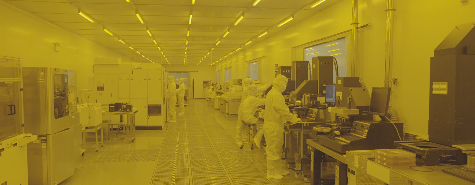
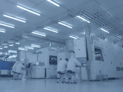
The Institute has established an advanced process service platform, and has put the world’s second and China’s first 6-inch advanced gallium arsenide device process production line into operation. It has a complete chip process system, including electron beam direct-write lithography machine, ordinary lithography machine, dry etching machine, magnetron sputtering coating machine, electron gun evaporation coating machine, etc., and can provide edge emitting laser based on various compound semiconductor materials such as GaAs, InP and GaN, VCSEL, photoelectric detector and other kinds of edge-emitting and surface-emitting laser and detector process services.
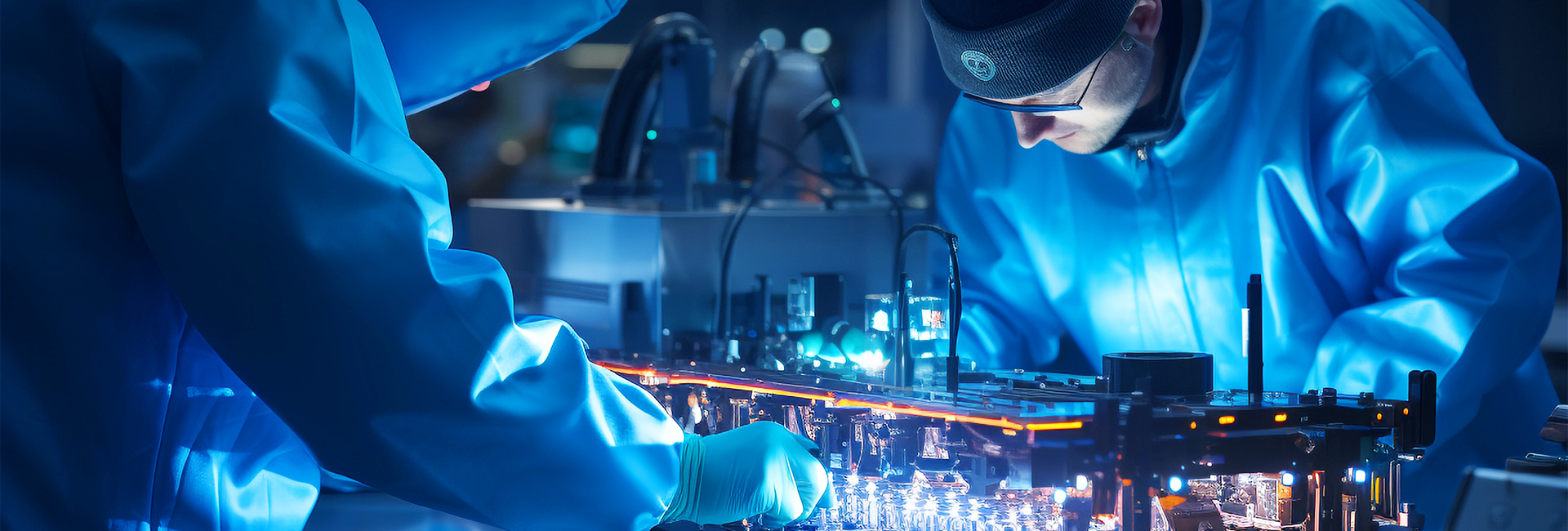
The Institute has constructed a unique photoelectric device packaging platform, equipped with SMT machine, vacuum reflow soldering and aging equipment packaging and welding system, able to provide TO, COS and other common semiconductor laser packaging testing and aging services.