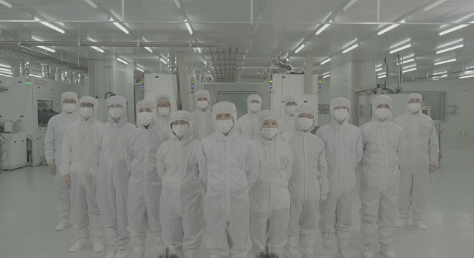

The center has several sets of research and development equipment for compound semiconductor and laser chip epitaxy, wafer process, cleavage coating, testing, analysis and packaging. It has a design and process expert team in the field of compound semiconductor and photoelectric device, serving several industrial technology fields such as photoelectricity and radio frequency and guiding compound semiconductor device and circuit design projects. The concept verification center promotes and encourages all related parties to actively contribute resources in a collaborative innovation way, motivates the teams to utilize resources, and more effectively run cross the “Innovation Death Valley”.
The concept verification center will incubate a series of compound semiconductor and photoelectric device enterprises with leading technical advantages, and promote the regional and even China’s technological improvement and industrial growth in the field of compound semiconductor and laser chip. Meanwhile, as the concept verification center is constructed, it will be firstly started in the Taihu Lake Photon Center’s compound semiconductor platform, serving some main fields of the photon industry. In the future, the compound photoelectron process level will also better meet the needs of all parties under the guidance of project needs introduced by the concept verification center, and the open technology research and development platform will be better positioned.
The concept verification center will incubate a series of compound semiconductor and photoelectric device enterprises with leading technical advantages, and promote the regional and even China’s technological improvement and industrial growth in the field of compound semiconductor and laser chip. Meanwhile, as the concept verification center is constructed, it will be firstly started in the Taihu Lake Photon Center’s compound semiconductor platform, serving some main fields of the photon industry. In the future, the compound photoelectron process level will also better meet the needs of all parties under the guidance of project needs introduced by the concept verification center, and the open technology research and development platform will be better positioned.