2023-09-15 Author: Everbright Institute Views: Loading
Conference on Industry-University-Research Cooperation in Jiangsu-Branch in High-tech Zone Suzhou Everbright Photonics Semiconductor Laser Innovation Research Institute Co., Ltd. participated in the release of the instrument and equipment sharing platform
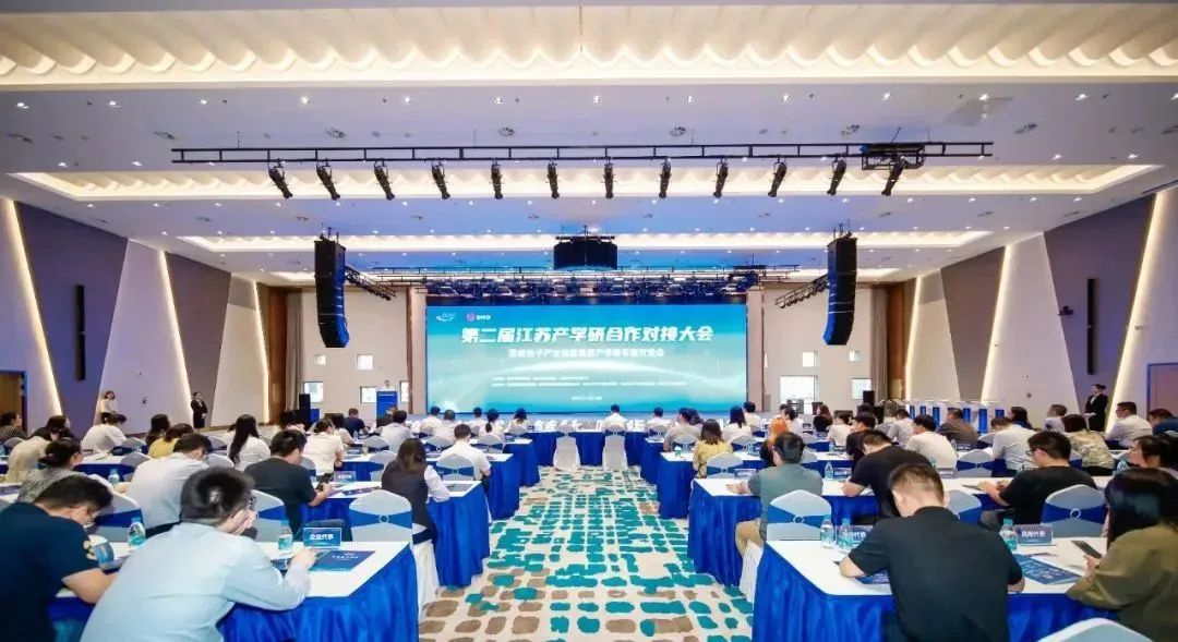
On September 14, 2023, the 2nd Conference on Industry-University-Research Cooperation in Jiangsu, namely Special Conference on University-Research Cooperation in Suzhou photon industry Innovation Cluster Industry, was successfully held in Suzhou High-tech Zone. As a major participant and carrier of Suzhou photon industry Innovation Cluster, Suzhou Everbright Photonics Semiconductor Laser Innovation Research Institute Co., Ltd. was invited to attend the conference and participate in the release of Instrument and Equipment Sharing Platform for photon industry in Suzhou High-tech Zone, and accepted the plate for Major Laboratory of Semiconductor Laser and Sensing in Jiangsu.
The construction of Suzhou photon industry Innovation Cluster is an important strategic measure advanced by the Suzhou Government. It focuses on the original innovation and transformation of achievements in the photon field, coordinates the resources related to Suzhou's photon industry, and promotes the construction of photon industry innovation clusters. Suzhou Semiconductor Laser Innovation Research Institute is an important innovation carrier of Suzhou Photonics Innovation Cluster.
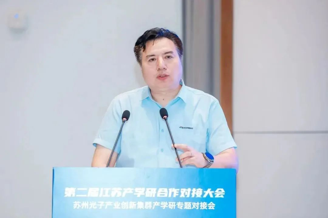
At the special conference, Li Shunfeng, Executive Vice President of Suzhou Semiconductor Laser Innovation Research Institute, shared the experience of Suzhou Everbright Photonics Co., Ltd. in promoting industry-university-research cooperation based on Suzhou High Power Semiconductor Laser Innovation Consortium. The Consortium, led by Everbright Photonics, is the first group of innovation consortium in Suzhou. It has delivered fruitful results in the field of industry-university-research cooperation and provided valuable experience for the construction of future innovation consortium.
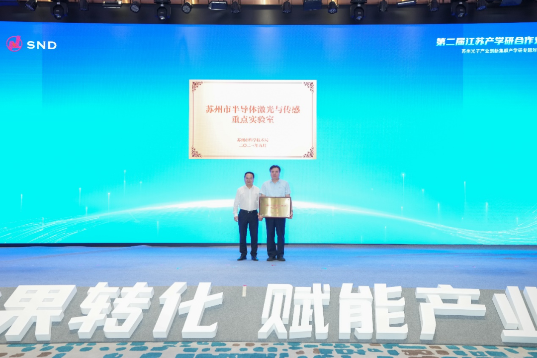
Award the Plate for Major Laboratory of Semiconductor Laser and Sensing in Jiangsu
The ceremony was held to award the plate for major laboratories in Suzhou. Gu Wanyong, Deputy Director of the Suzhou Science and Technology Bureau, awarded the plate for Major Laboratory of Semiconductor Laser and Sensing in Jiangsu built as guided by Everbright Photonics. Such Laboratory aims at major national strategic needs, relies on Everbright Photonics and Suzhou Semiconductor Laser Innovation Research Institute in terms of technology and industry, and focuses on major and cutting-edge technologies in the field of semiconductor laser and sensing technology to carry out project research. Such Laboratory is built in order to further improve the key parameters such as brightness, power and band of semiconductor lasers, and to solve the key scientific and technological problems in the development of semiconductor lasers and photodetectors. As a result, technical support will be provided for localized high-end semiconductor optoelectronic devices, and China’s sustainable innovation capabilities in this field enhanced.
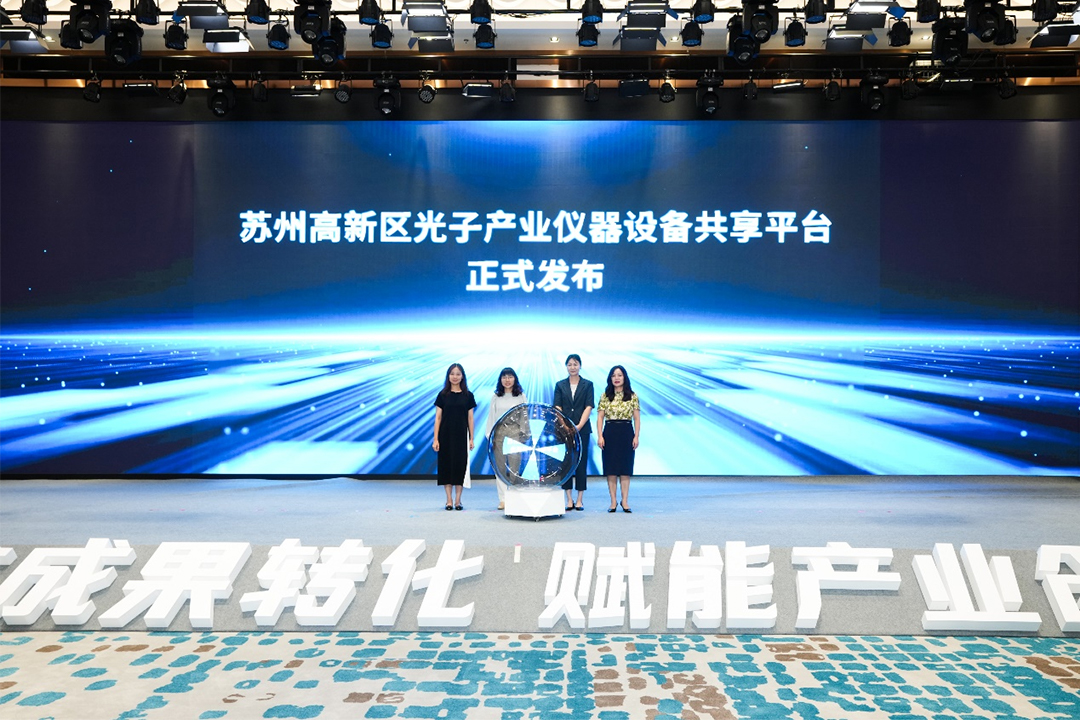
Participated in the release of instrument and equipment sharing platform for the photon industry in Suzhou High-Tech Zone
At the conference, the platform was officially released. The platform provides small and medium-sized enterprises with epitaxial material testing, chip process development, device packaging and testing and other services, helps enterprises quickly find corresponding testing service institutions, and helps enterprises in photon industry grow rapidly. Suzhou Semiconductor Laser Innovation Research Institute is an important participant of this platform. The Institute has complete instruments and equipment to provide testing and process development services in compound semiconductors and related fields, including (not limited to) material and device testing and analysis, epitaxial process services, chip process services, optoelectronic device packaging, etc. Everbright Photonics has built the advanced 6-inch GaAs optoelectronic device process production line, which is one of only two such production lines in the world and is also the only one in China. It has strong capabilities in testing and process service, and will continue to contribute an important force to the development of Suzhou's photon industry in the future.
As a research and innovation platform built by Everbright Photonics, Suzhou Semiconductor Laser Innovation Research Institute, makes full use of Everbright Photonics' internationally top platform for chip R&D and manufacturing process, and is committed to cultivating and introducing a group of high-level talents and industrialization projects related to the field of semiconductor lasers and optoelectronics, so as to make it a specialized platform to incubate and industrialize achievements made in the field of semiconductor laser and other semiconductor optoelectronic device, and also an internationally influential highland and industrial base for scientific and technological innovation in semiconductor laser chip and related fields.
Conference on Industry-University-Research Cooperation in Jiangsu
The 2nd Conference on Industry-University-Research Cooperation in Jiangsu was sponsored by the Jiangsu Provincial Department of Science and Technology. Aiming at "promoting the transformation of scientific and technological achievements and empowering industrial innovation and development", the conference released more than 600 latest scientific and technological achievements on the spot, and linked the entities in terms of more than 1000 technology transfer demands from enterprises, to help transfer transform and industrialize a number of cutting-edge scientific and technological achievements in Jiangsu.The construction of Suzhou photon industry Innovation Cluster is an important strategic measure advanced by the Suzhou Government. It focuses on the original innovation and transformation of achievements in the photon field, coordinates the resources related to Suzhou's photon industry, and promotes the construction of photon industry innovation clusters. Suzhou Semiconductor Laser Innovation Research Institute is an important innovation carrier of Suzhou Photonics Innovation Cluster.
At the special conference, Li Shunfeng, Executive Vice President of Suzhou Semiconductor Laser Innovation Research Institute, shared the experience of Suzhou Everbright Photonics Co., Ltd. in promoting industry-university-research cooperation based on Suzhou High Power Semiconductor Laser Innovation Consortium. The Consortium, led by Everbright Photonics, is the first group of innovation consortium in Suzhou. It has delivered fruitful results in the field of industry-university-research cooperation and provided valuable experience for the construction of future innovation consortium.
Award the Plate for Major Laboratory of Semiconductor Laser and Sensing in Jiangsu
Participated in the release of instrument and equipment sharing platform for the photon industry in Suzhou High-Tech Zone
As a research and innovation platform built by Everbright Photonics, Suzhou Semiconductor Laser Innovation Research Institute, makes full use of Everbright Photonics' internationally top platform for chip R&D and manufacturing process, and is committed to cultivating and introducing a group of high-level talents and industrialization projects related to the field of semiconductor lasers and optoelectronics, so as to make it a specialized platform to incubate and industrialize achievements made in the field of semiconductor laser and other semiconductor optoelectronic device, and also an internationally influential highland and industrial base for scientific and technological innovation in semiconductor laser chip and related fields.