2022-11-29 Author: Everbright Institute Views: Loading
Powerful Combination “Gallium Nitride Laser Joint Laboratory” of Suzhou Semiconductor Laser Innovation Institute and Suzhou Institute of Nano-Tech and Nano-Bionics (SINANO), Chinese Academy of Sciences is unveiled and established
On the morning of November 29, “Gallium Nitride Laser Joint Laboratory” of Suzhou Semiconductor Laser Innovation Institute and Suzhou Institute of Nano-Tech and Nano-Bionics (SINANO), Chinese Academy of Sciences was officially unveiled and established in Suzhou Everbright Photonics Co., Ltd. Wu Xuxiang, Vice Director of Suzhou New District Management Committee and Deputy District Mayor, Yang Liang, Deputy Secretary of Party Working Committee and Director of Management Committee of Science and Technology Town, Li Wei, Director of Science and Technology Bureau of Suzhou New District, Deng Qiang, Secretary of the Party Committee of SINANO, Ji Xiaoyan, Director of Technology Transfer Center, Liu Jianping, researcher, Min Dayong, Chairman, Wang Jun, President and Li Shunfeng, Executive Vice-President of Suzhou Semiconductor Laser Innovation Institute attended the activity.
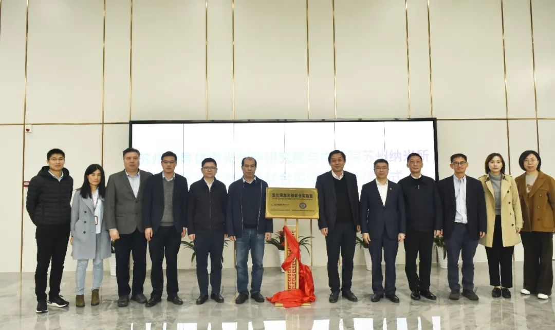
Opening ceremony of Gallium Nitride Laser Joint Laboratory
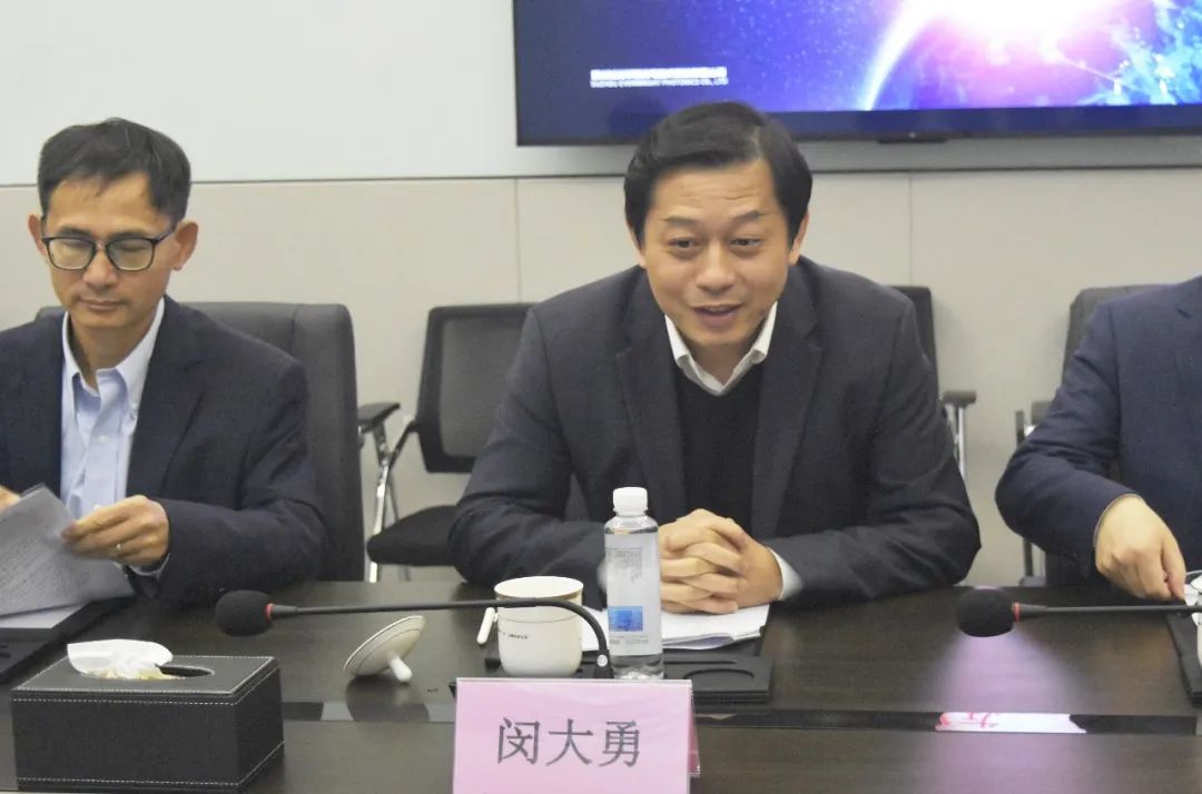
Min Dayong, Chairman of Suzhou Semiconductor Laser Innovation Institute
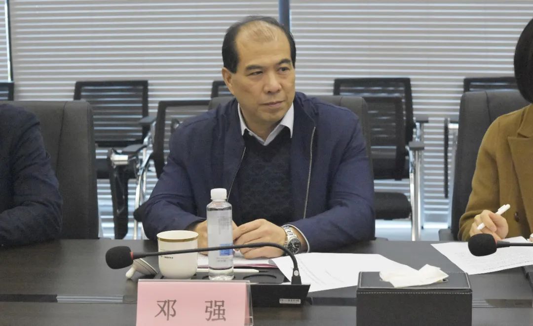
Deng Qiang, Secretary of the Party Committee of Suzhou Institute of Nano-Tech and Nano-Bionics (SINANO), Chinese Academy of Sciences
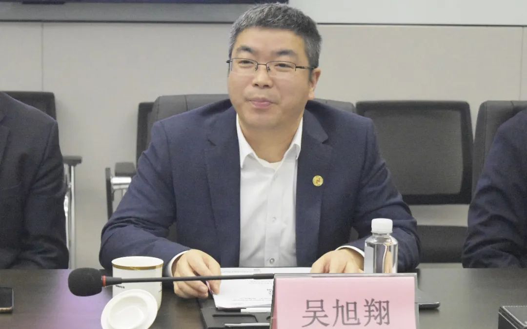
Wu Xuxiang, Vice Director of Suzhou New District Management Committee and Deputy District Mayor
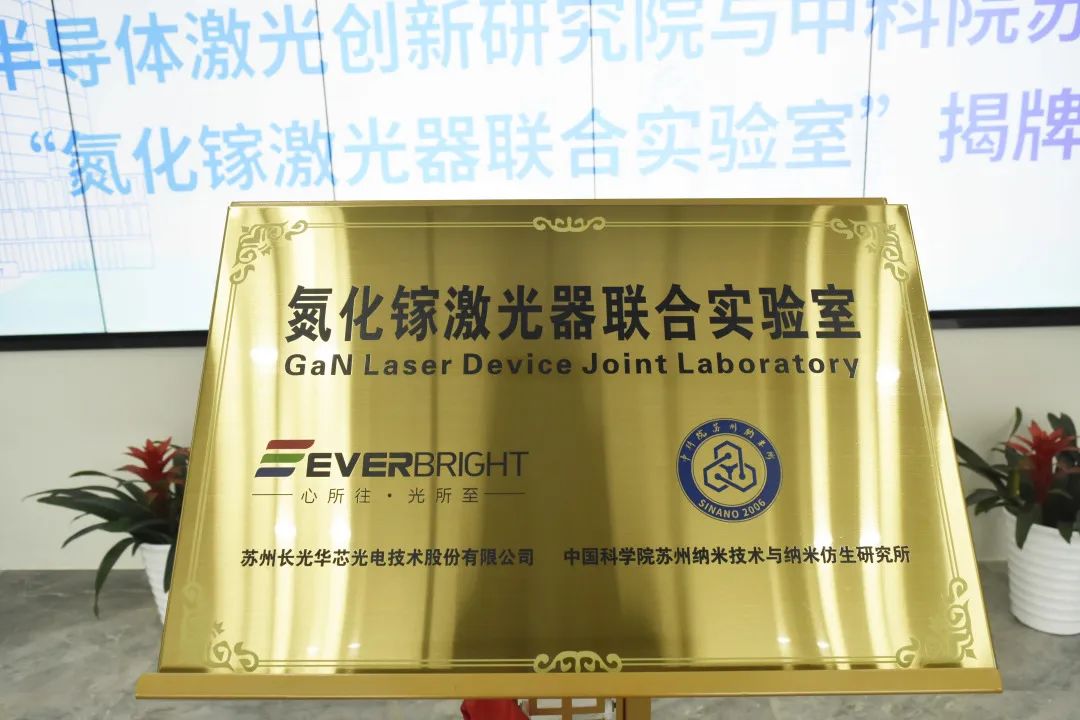
Gallium Nitride Laser Joint Laboratory
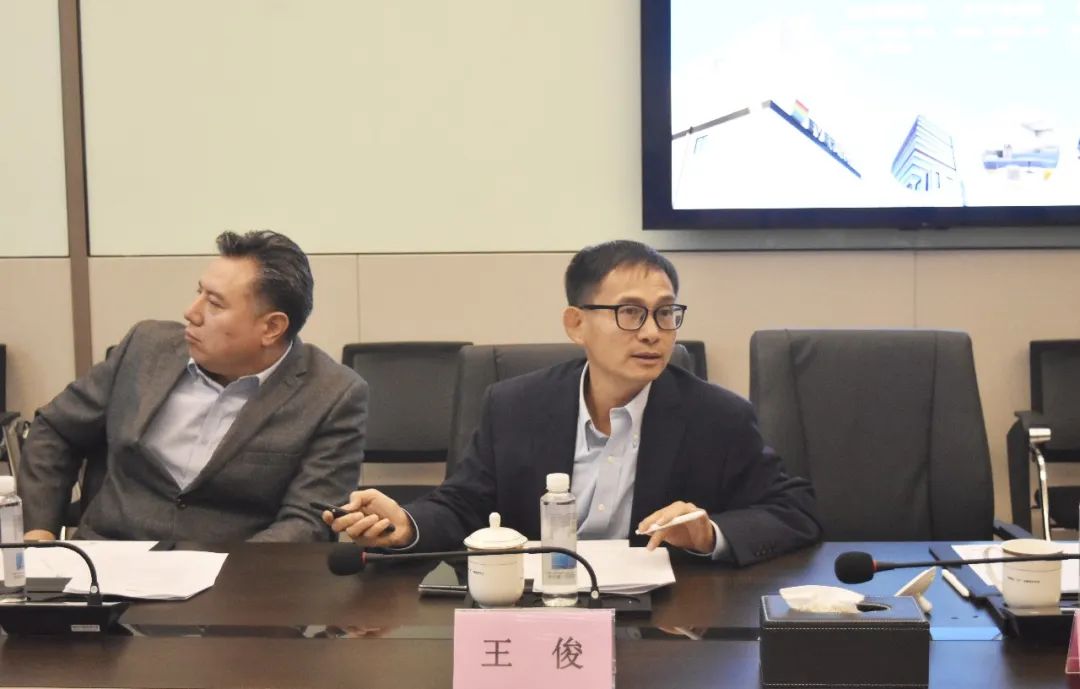
Wang Jun, President of Suzhou Semiconductor Laser Innovation Institute
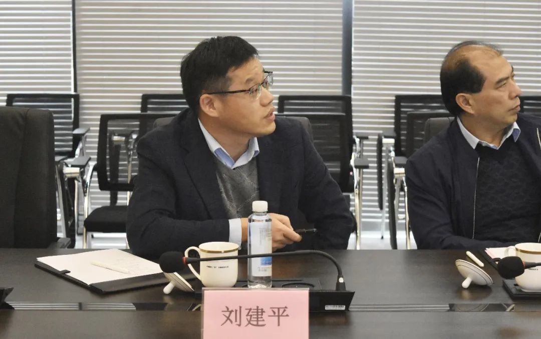
Liu Jianping, researcher of Suzhou Institute of Nano-Tech and Nano-Bionics (SINANO), Chinese Academy of Sciences
In the future, Suzhou Semiconductor Laser Innovation Institute will continue to increase its resource investment in gallium nitride laser chip to obtain the momentum and energy of sustainable development. It will also take the joint laboratory as the opportunity to further upgrade the partnership, continuously expand and extend product technology cooperation field and consolidate the cornerstone and source of China's laser industry chain.
Opening ceremony of Gallium Nitride Laser Joint Laboratory
Min Dayong, Chairman of Suzhou Semiconductor Laser Innovation Institute
Min Dayong, Chairman of Suzhou Semiconductor Laser Innovation Institute delivered a speech and expressed, the unveiling and establishment of “Gallium Nitride Laser Joint Laboratory” were of great significance. Everbright Photonics was in the rapid development stage after listing and the establishment of the “Joint Laboratory” meant an important horizontal business expansion by the Institute focusing on the core semiconductor laser field, extending the existing core semi-conductor laser of the company from short-wave infrared and near-infrared fields to visible light field. Our partner, Suzhou Institute of Nano-Tech and Nano-Bionics (SINANO), Chinese Academy of Sciences, had more than ten years of deep research basis in gallium nitride laser. We believed that, by taking the advantage of industrial innovation cluster construction of “Taihu Lake Photon Center”, our cooperation represented the win-win cooperation of “east nano” and “west photon” and would yield positive results in the future, filling in another domestic technology gap, realizing the domestication of laser chip of another application field from source and promoting the booming of photon industry.
Deng Qiang, Secretary of the Party Committee of Suzhou Institute of Nano-Tech and Nano-Bionics (SINANO), Chinese Academy of Sciences
Deng Qiang, Secretary of the Party Committee of SINANO, delivered a speech and expressed, to develop semi-conductor and photoelectron, both R&D ability and region clustering were required. SINANO had always focused on national major demands since its establishment, but was characterized by strong technology and weak system. Everbright Photonics had an excellent scientific research platform and was keenly sensitive to market demands, which was typical for scientific research project industrialization. From the perspective of region gathering, Suzhou has a good scientific research and industrial base. It was expected, technical research capabilities in the front-end and technology, process and quality level in the back-end would be strengthened through the establishment of joint laboratory and focusing on national key demands. Directional technology research could be guided through market demands and product level could be promoted through front-end technology breakthrough to form a benign circle, promote market traction and achievement transformation and create the strongest innovation consortium!
Wu Xuxiang, Vice Director of Suzhou New District Management Committee and Deputy District Mayor
Wu Xuxiang, Vice Director of Suzhou New District Management Committee and Deputy District Mayor of Huqiu District, delivered a speech and expressed, at present, Suzhou New District was making every effort to build a world-class photon innovation center and create a photon industry innovation cluster at one hundred billion level. Affected by great power competition, technological change and COVID-19 pandemic, security and stability of the industrial chain were more emphasized in photoelectronic industry. SINANO and Suzhou Semiconductor Laser Innovation Institute summed up scientific problems based on industrial demands, established a joint innovation body for industrial scientific research and completed each other’s advantages to jointly establish “Gallium Nitride Laser Joint Laboratory”, which would strongly promote the combination and mutual complementarity of “east nano” and “west photon” in high-end innovative resources and create a template example of the construction of “Taihu Lake Photon Center”.
Gallium Nitride Laser Joint Laboratory
Gallium Nitride is a representative material system in the third-generation semi-conductor and gallium nitride-based blue-green laser has huge application advantages and irreplaceable roles in many fields, such as laser display, non-ferrous metal processing etc. Because gallium nitride-based blue-green laser is a key product with the greatest technical difficulty and industrial height in the third-generation semi-conductor photoelectric devices, it is still blank in China.
Relying on the stronger competitive advantages of the Institute and SINANO in photoelectric devices, semi-conductor materials, micro and nano fabrication and other fields, Gallium Nitride Laser Joint Laboratory, through the understanding and recognition of Everbright towards the industry, led by the cutting-edge physical basis and technical research of gallium nitride laser, integrates the discipline strength of SINANO, overcomes difficulties, jointly concentrates and cooperates to carry out oriented research in related directions, firstly fills in the blank of China in third-generation semi-conductor optoelectronic device fields, such as gallium nitride-based blue-green laser and constructs an integral and leading laser industry chain in China with all its might.
Wang Jun, President of Suzhou Semiconductor Laser Innovation Institute
Wang Jun, President of Suzhou Semiconductor Laser Innovation Institute, introduced the overall thought of the construction of the Institute and the plan supporting the construction of Taihu Lake Photon Center. The Institute adheres to the development strategy of “one platform, one support point, horizontal expansion and vertical extension”, expands businesses and invests in incubation around optoelectronics and compound semiconductors. At present, the company has three material systems, namely gallium arsenide system, indium phosphide system and gallium nitride system, R&D capability of 2-inch GaN laser and production lines of 3-inch indium phosphide and 6-inch gallium arsenide laser. In the future, Everbright will create a R&D and industrialization platform of advanced devices developed based on the material, process and packaging technique of photoelectric and electronic devices of multicompound semiconductor. After the platform is built, the company’s laser chip and device production ability will achieve a qualitative leap. The R&D and process platform has R&D and production capacity of all-series compound semiconductor devices. Based on the internationally leading 6-inch compound production line, it promotes its R&D hardware conditions and R&D production level to reach the international top and has the import substitution ability of domestic devices and modules in many fields. It endeavors to build a new industrial ecological chain with laser localization in China where governments, capitals, industry, areas, the Institute are interconnected with enterprises, upstream and downstream innovation synergy, supply chain and promotes the innovative development of laser industry technology in China.
Liu Jianping, researcher of Suzhou Institute of Nano-Tech and Nano-Bionics (SINANO), Chinese Academy of Sciences
Liu Jianping, researcher of Suzhou Institute of Nano-Tech and Nano-Bionics (SINANO), Chinese Academy of Sciences introduced the future work plan of Gallium Nitride Laser Joint Laboratory. SINANO team has been working for more than ten years, and has firstly researched gallium nitride blue and green lasers in China. The joint laboratory integrates the R&D team and technology ability of SINANO, the internationally leading whole-process platform and production line of laser chip IDM of Everbright, which can be called powerful combination. It will break the reliance on imports for gallium nitride laser chip and strive to make Taihu Lake Photon Center the first place for localization of gallium nitride laser chip.
In the future, Suzhou Semiconductor Laser Innovation Institute will continue to increase its resource investment in gallium nitride laser chip to obtain the momentum and energy of sustainable development. It will also take the joint laboratory as the opportunity to further upgrade the partnership, continuously expand and extend product technology cooperation field and consolidate the cornerstone and source of China's laser industry chain.